
Established: July 1992
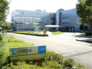
Location: 10 Okubo, Tsukuba-shi, Ibaraki-pref.
Area: 38,311m2
At the Tsukuba Laboratory, the main focus of research and development are the both researches of basic technology and new product development on the gas and equipment for the fields of electronics. Examples of R&D themes related to the electronics materials and equipment include those such as the ultra-clean technology and trace gas analysis for the highly purified gas supply, and the development of the compound semi-conductor manufacturing devices. The laboratory is equipped with the class 100 clean room and the state-of-the-art MOCVD systems and the researchers are actively interacting with the other R&D laboratories and the national institutions around Tsukuba area, like conducting the joint research. Especially the development of GaN-MOCVD system that produces the materials for the recent hot-topic blue LED is attracting a lot of attention. Tsukuba laboratory is used not only for the research and development purpose, but also for other purposes that fulfill the main needs of TAIYO NIPPON SANSO's Electronics Department. Such as the gas laboratory for the quality-control analysis, and is expected to expand the capability to develop the breakthrough innovations that drive the future growth in the rapid growing market.
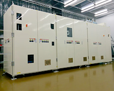
MOCVD
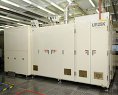
GaN Mass Production MOCVD UR25K
4"x10 or 6"x7
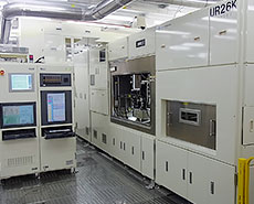
GaN Mass Production MOCVD UR26K
6"x10 or 8"x6
GaN R&D-Production MOCVD SR-4000HT
2"x3 or 4"x1
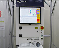
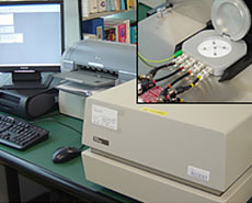
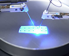
Evaluation tool
Optical Microscope
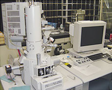
FE-SEM
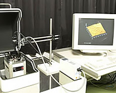
AFM
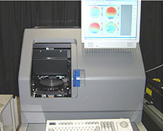
PL Mapping System
Hall Effect Measurement System
EL Measurement System
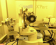
X-ray Diffraction System